3.3.Synchronous Digital Systems
\(3.3.\)Synchronous Digital Systems
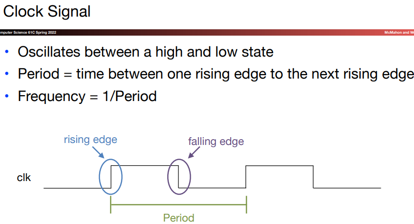
1.Clock concepts
2.D Flip-flops
\(a.\) DFF concept
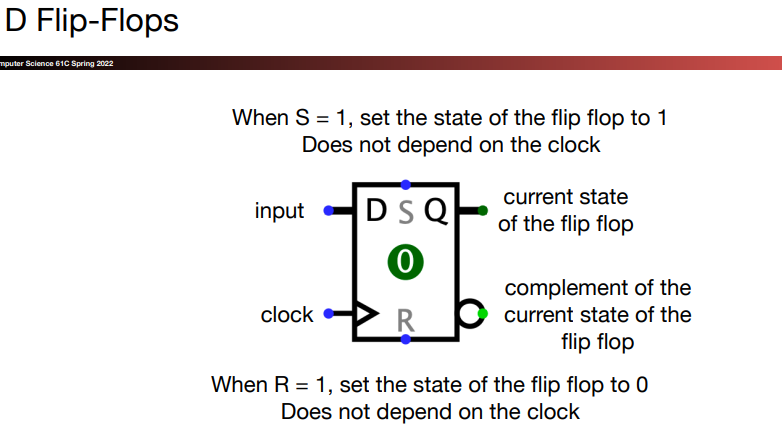
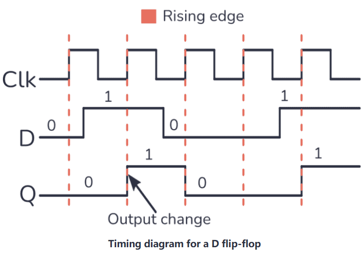
The \(Q\) is the output of DFF, the \(D\) is the data input.
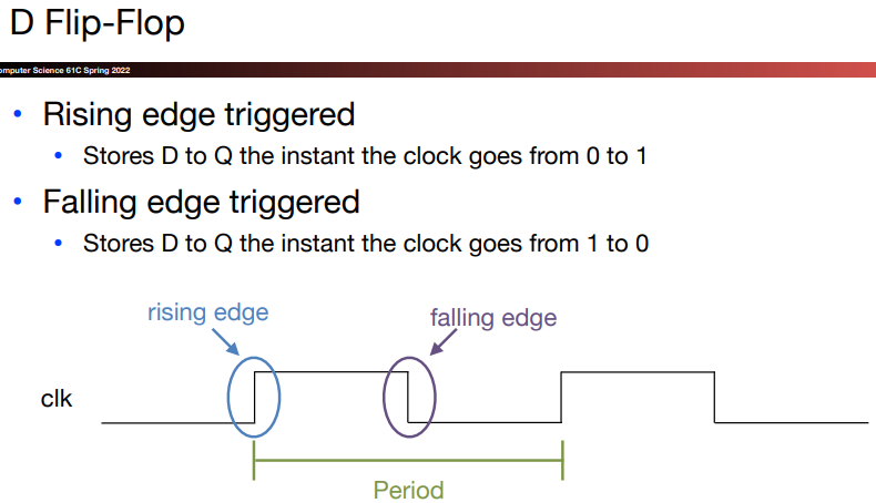
DFF only responds to the input signal on the rising edge of the clock signal, it captures and latches the value of data input. It will hold the value until the next rising edge of the clock signal.
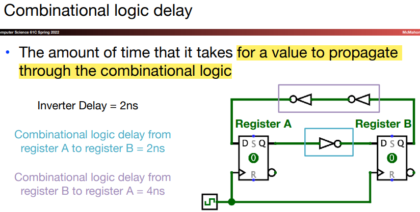
Clock-to-Q delay is the amount of time that it take for the input to propagate to the output after the clock trigger.
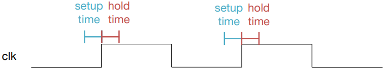
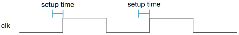
Setup time is the amount of time that the input needs to be stable BEFORE the clock trigger
- Hold time is the amount of time that the input needs to be stable AFTER the clock trigger
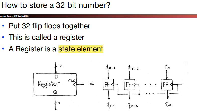
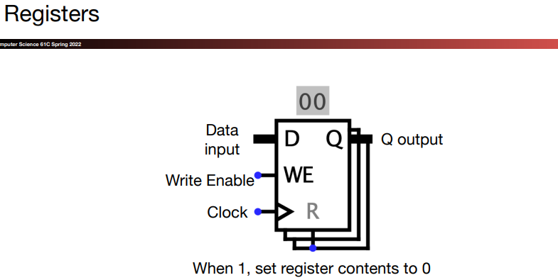
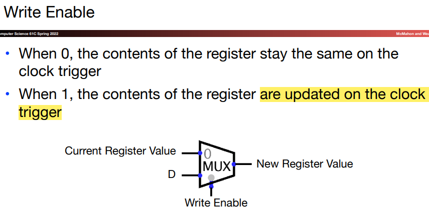
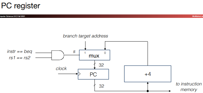
3.Register
\(a.\)Some concept
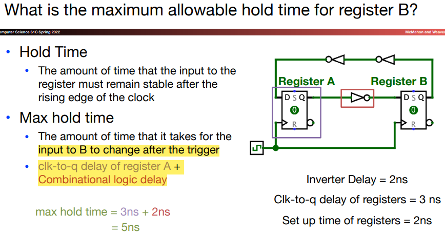
Why this? Because the max hold time is to ensure that data input D remains stable for a period of time after the rising edge of the clock arrives. And the period of time equals to the delay of \(A\) plus the combinational delay.
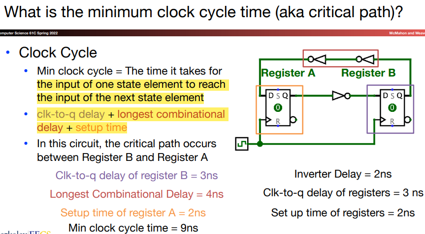
Why this? Because the min clock cycle is to ensure that the signal is properly transmitted during the clock cycle and captured by the next register. So we must take the longest time into consideration.
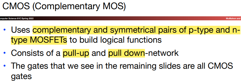
4.Transitor
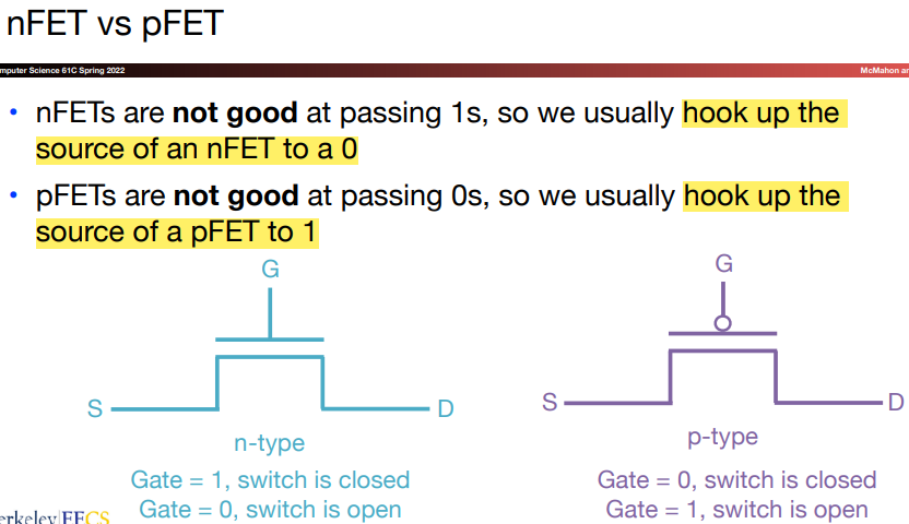
\(a.\)Metal-Oxide Semiconductor Field Effect Transistor(MOSFET)
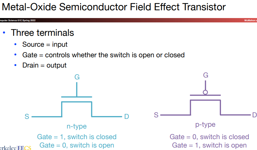
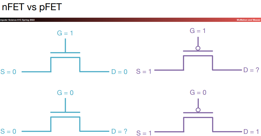
To know how the result comes from, we can view the value of \(S\), \(G\) and \(D\) as the voltage. Take this as an example:
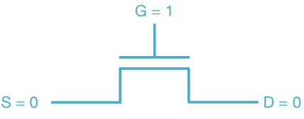
First we need to know whether the switch is closed. If the switch is closed, then the state of \(D\) is decided by the outside circuits.
When the switch is on, we then judge if the voltage of \(S\) is higher than that of \(G\). If it's true, then the FET is conducting, and vice versa.
In this example, the voltage of \(S\) is lower than \(G\), so the \(D\) can't get the electronic, thus it's 0.
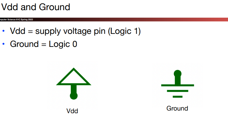
\(b.\)Vdd and Ground
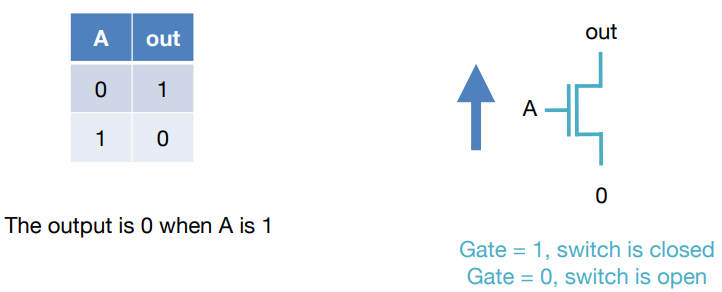
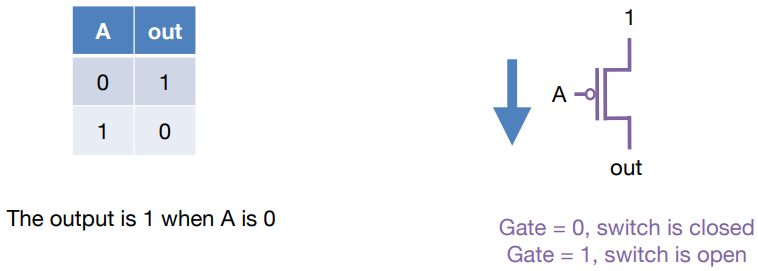
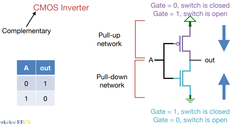
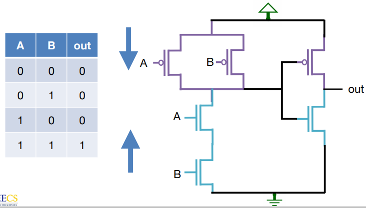
\(c.\)Building an Inverter
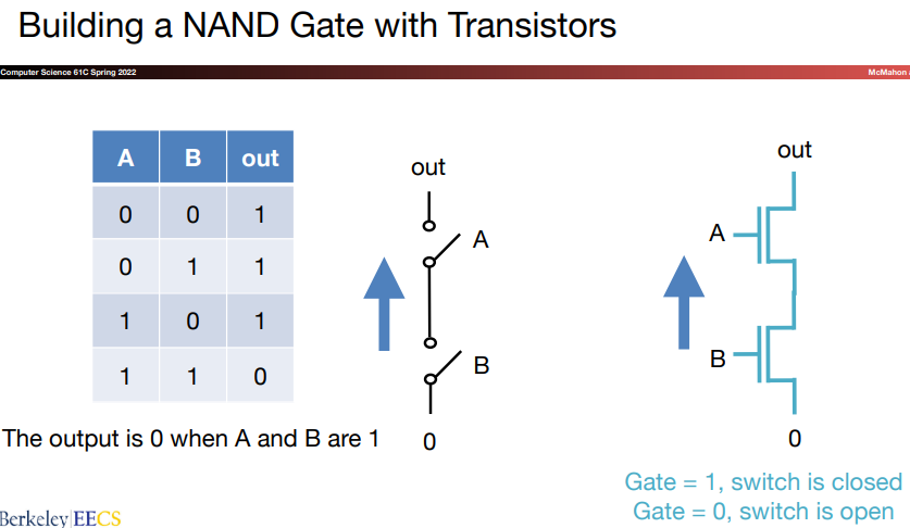
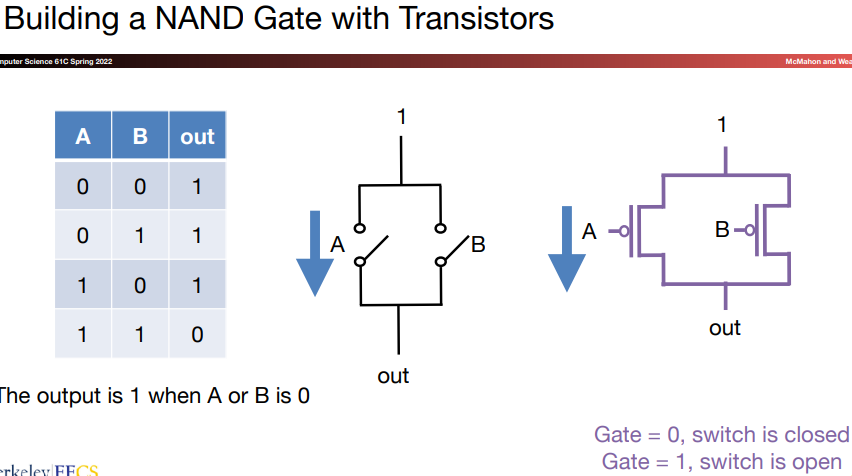
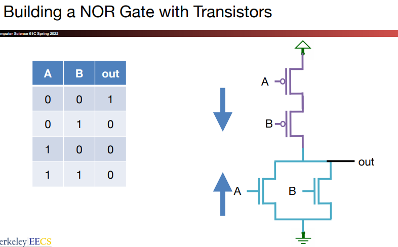
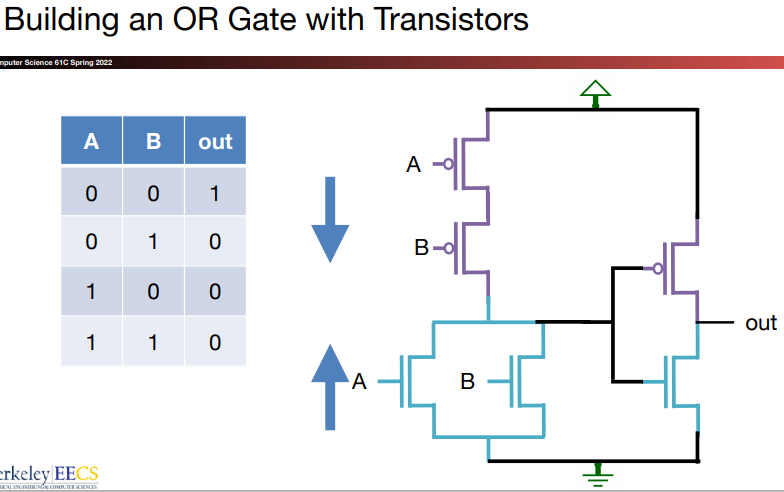
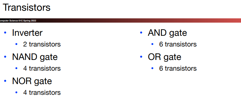
\(d.\)Building other gates
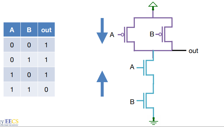
To build a CMOS, we:
Implement the pull-up network and pull-down network separately to fit the truth table.
- It's OK to get the opposite of truth table. We can simply convert it through an invertor.
Connect the pull-up with Vdd, and the pull-down with Ground.
We take the NAND gate for example:
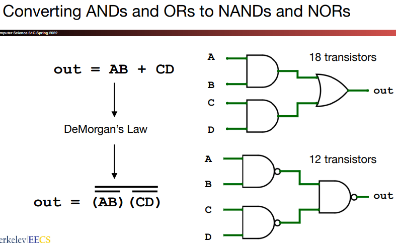
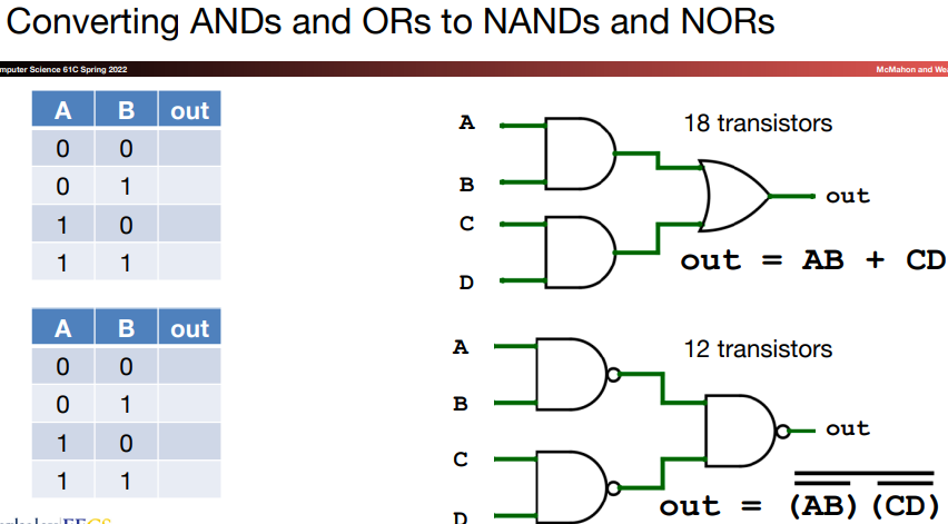
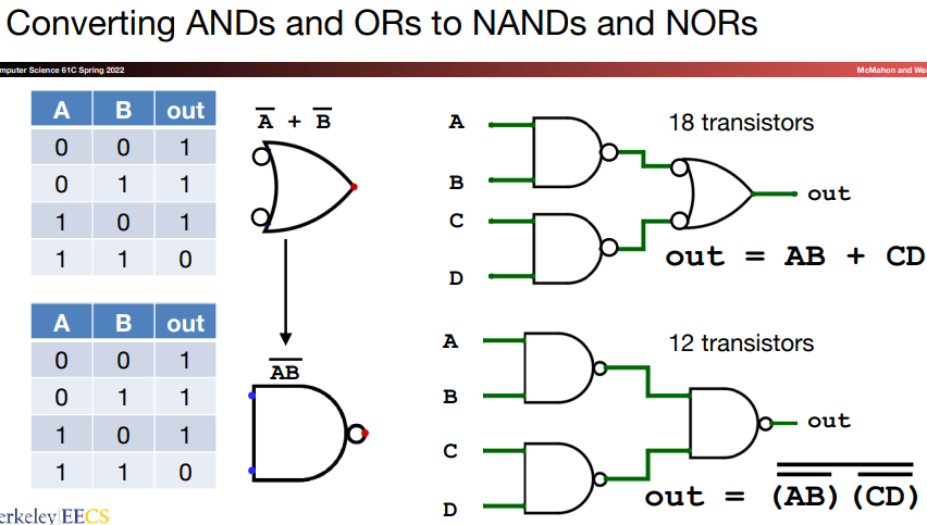
\(e.\)The use of DeMorgan's Law