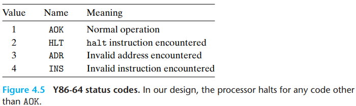
4.2.Logical Design and the HCL
\(4.2.\)Logical Design and the HCL
1.Combinational Circuits & HCL Boolean Expressions
By assembling a number of logic gates into a network, we can construct computational blocks known as combinational circuits. There are several restrictions:
Every logic gate input must be connected to exactly one of the following:
one of the system inputs (known as a primary input)
the output connection of some memory element
the output of some logic gate.
The outputs of two or more logic gates cannot be connected together. Otherwise, the two could try to drive the wire toward different voltages, possibly causing an invalid voltage or a circuit malfunction.
The network must be acyclic. That is, there cannot be a path through a series of gates that forms a loop in the network.
The following shows an example of a combinational circuit:
The network is written in HCL as:
1 | bool eq = (a && b) || (!a && !b) |
The HCL uses C-sytle syntax. However, we don't view the code as performing a computation and assigning the result to some memory location. Instead, it is simply a way to give a name to an expression.
There are some other differences that are worth noting:
The combinational circuit has the property that the outputs continually respond to changes in the inputs. By contrast, a C expression is only evaluated when it is encountered during the execution of a program.
The combinational circuit only operates over the bit value 0 and 1.
Logical expressions in C have the property that they might only be partially evaluated. If the outcome of an and or or operation can be determined by just evaluating the first argument, then the second argument will not be evaluated. In contrast, combinational logic doesn't have any partial evaluation rules.
2.Word-Level Combinational Circuits and HCL Integer Expression
Combinational circuits that perform word-level computations are constructed using logic gates to compute the individual bits of the output word, based on the individual bits of the input words. The following circuit tests if two words A and B are equal:
HCL allows words to be compared for equality. So we can express the
circuit as bool Eq = (A == B)
Multiplexing functions are described in HCL using casing expressions. A case expressions has the following general form:
\[ \begin{bmatrix} \text{select}_1 : \text{expr}_1; \\ \text{select}_2 : \text{expr}_2; \\ \vdots \\ \text{select}_k : \text{expr}_k; \end{bmatrix} \]
\(select_i\) indicates when this case should be selected.
The integer expression \(expr_i\) indicates the resulting value.
The selection expressions can be arbitrary Boolean expressions, and there can be an arbitrary number of cases.
Logically, the selection expressions are evaluated in sequence, and the case for the first one yielding 1 is selected.
For example, the figure below shows the circuit of the word-level multiplexor:
it can be expressed in HCL as:
1 | word Out = [ |
And a 4-way multiplexor can be expressed in HCL as:
1 | word Out4 = [ |
If we want to design a logic circuit that finds the minimum value among a set of words A, B and C, we can write the following HCL program:
1 | word MIN3 = [ |
3.Set Membership
The general form of a set membership test is:
\[ \text{iexpr} \in \{\text{iexpr}_1, \text{iexpr}_2, \ldots, \text{iexpr}_k\} \]
where the value being tested(\(iexpr\)) and the candidate matches(\(iexpr_1\) through \(iexpr_k\)) are all integer expressions.
4.Memory and Clock
\(a.\)Summary
Combinational circuits don't store any information, they simply react to the signals at their inputs. So we must introduce devices that store information represented as bits.
Our storage devices are all controlled by a single clock, a periodic signal that determines when new values are to be loaded into the devices.
We consider two classes of memory devices:
Clocked registers(simple registers): It stores individual bits or words. The clock signal controls the loading of the register with the value at its input.
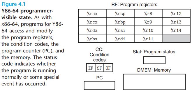
- Our Y86-64 processors will use clocked registers to hold the program counter(PC), the condition codes(CC), and the program status(Stat).
Random access memories(simply memories):It store multiple words, using an address to select which word should be read or written.
Examples of random access memories include
the virtual memory system of a processor, where a combination of hardware and operating system software make it appear to a processor that it can access any word within a large address space;
the register file, where register identifiers serve as the addresses.
In a Y86-64 processor, the register file holds the 15 program registers(
%raxthrough%r14).
In hardware, a register is directly connected to the rest of the circuit by its input and output wires. In machine-level programming, the registers represent a small collection of addressable words in the CPU, where the addresses consist of register IDs.
The following figure shows the detailed register operation:
In the figure, the register serves as barriers between the combinational logic in different parts of the circuit.
\(b.\)Register file
The following g diagram shows a typical register file:
The multiported RAM allows multiple read and write operations to take place simultaneously.
Each port has an address input, indicating which program register should be selected, and a data output or input giving a value for that program register.
Every time the clock rises, the value on input
valWis written to the program register indicated by the register ID on inputdstW.- When
dstWis set to0xF, no program register is written.
- When
\(c.\)Data memory
The Data memory is used to store program data:
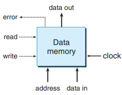
This memory has a single address input, a data input for writing, and a data output for reading.
We set
addressto the desired address,data into the desired value.The
errorsignal will be set to 1 if theaddressis out of range.