4.3.Sequential Y86-64 Implementation
\(4.3.\)Sequential Y86-64 Implementation
1.Organizing Processing into Stages
\(a.\)Summary
The following is an informal description of the stages and the operations performed within them:
Fetch: The fetch stage reads the bytes of an instruction from memory, using the program counter(PC) as the memory address.
From the instruction it extracts the two 4-bit portions of the instruction specifier byte, referred to as
icode(the instruction code) andifun(the instruction function).It computes
valPto be the address of the instruction following the current one in sequential order. That is,valPequals the value of the PC plus the length of the fetched instruction.
Decode: The decode stage reads up to two operands from the register file, giving values
valAand/orvalB.Execute: In the execute stage, the arithmetic/logic unit(ALU) either performs the operation specified by the instruction(according to the value of
ifun), computes the effective address of a memory reference, or increments or decrements the stack pointer. We refer to the resulting value asvalE.- For a conditional move instruction, the stage will evaluate the
condition codes and move condition (given by
ifun) and enable the updating of the destination register only if the condition holds.
- For a conditional move instruction, the stage will evaluate the
condition codes and move condition (given by
Memory: The memory stage may write data to memory, or it may read data from memory. We refer to the value read as
valM.Write Back: The write-back stage writes up to two results to the register file.
PC Update: The PC is set to the address of the next instruction.
In our simplified implementation, the processor will stop when any
exception occurs - that is, when it executes a halt or
invalid instruction, or it attempts to read or write an invalid
address.
\(b.\)Arithmetic operations
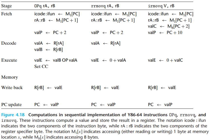
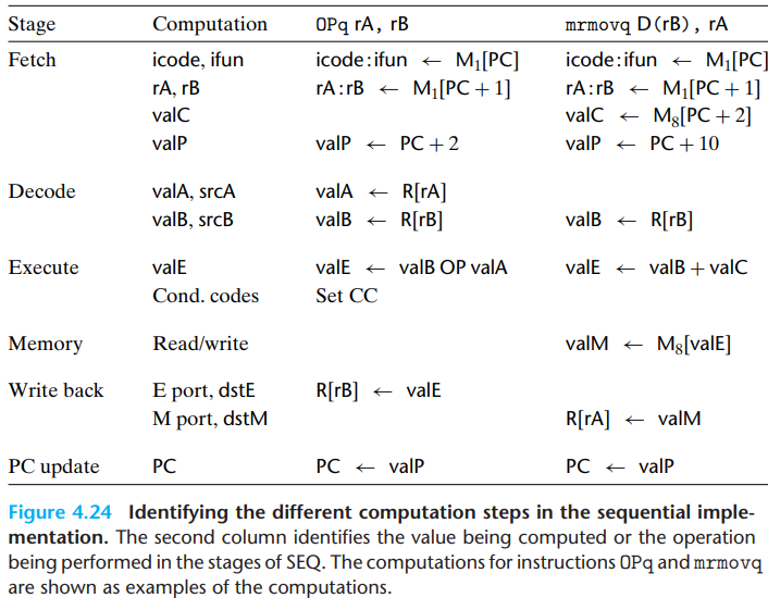
For the integer-operation instruction:
In the fetch stage, we do not require a constant word, and so
valPis computed asPC+2.During the decode stage, we read both operands. These are supplied to the ALU in the execute stage, along with the function specifier
ifun.valEequals to the instruction resultvalB OP valA. TheOPis specified byifun.
For the
rmmovqinstruction:The process is similar to integer-operation operation, but we don't need to fetch the second register operand. Instead, we set the second ALU input to zero and add this to the first, giving
valE = valA.In addition, we must increment the program counter by 10 for
irmovqdue to the long instruction format.
\(c.\)Operations involving memory operation
The following instructions involve memory write and read stage:
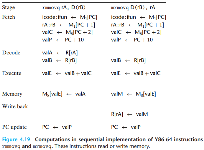
The process use the ALU to add
valCtovalB, giving the effective address for memory operation.In the memory stage, we either write the register value
valAto memory or readvalMfrom memory.
\(d.\)pushq &
popq operations
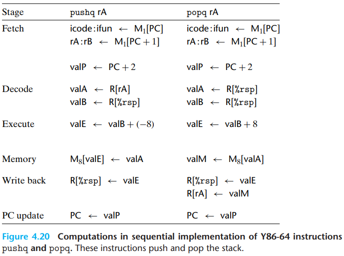
The pushq and popq involve both accessing
memory and incrementing or decrementing the stack pointer.
For the
pushqinstruction:In decode stage, we use
%rspas the identifier for the second register operand, giving the stack pointer asvalB.In the execute stage, we use the ALU to decrement the stack pointer by 8. This decremented value is used for the memory write address and is also stored back to
%rspin the write-back stage.We use
valEas the address for the write operation.
we adhere to the Y86-64 convention that
pushqshould decrement the stack pointer before writing.
For the
popqinstruction:The
popqinstruction proceeds much likepushq, except that we read two copies of the stack pointer in the decode stage. This is clearly redundant, but we will see that having the stack pointer as bothvalAandvalBmakes the subsequent flow more similar to that of other instructions, enhancing the overall uniformity of the design.We use the unincremented value as the address for the memory operation.
In the write-back stage, we update both the stack pointer register with the incremented stack pointer and register
rAwith the value read from memory.
\(e.\)Control transfer instructions
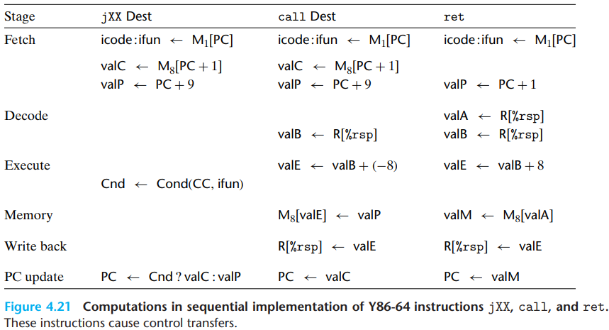
A jump instruction proceeds through fetch and decode much like the previous instructions, except that it does not require a register specifier byte.
In the execute stage, we check the condition codes and the jump condition to determine whether or not to take the branch, yielding a 1-bit signal
Cnd.We test this flag and set the PC to
valC(the jump target) if the flag is 1 and tovalP(the address of the following instruction) if the flag is 0.
\(f.\)call &
ret operations
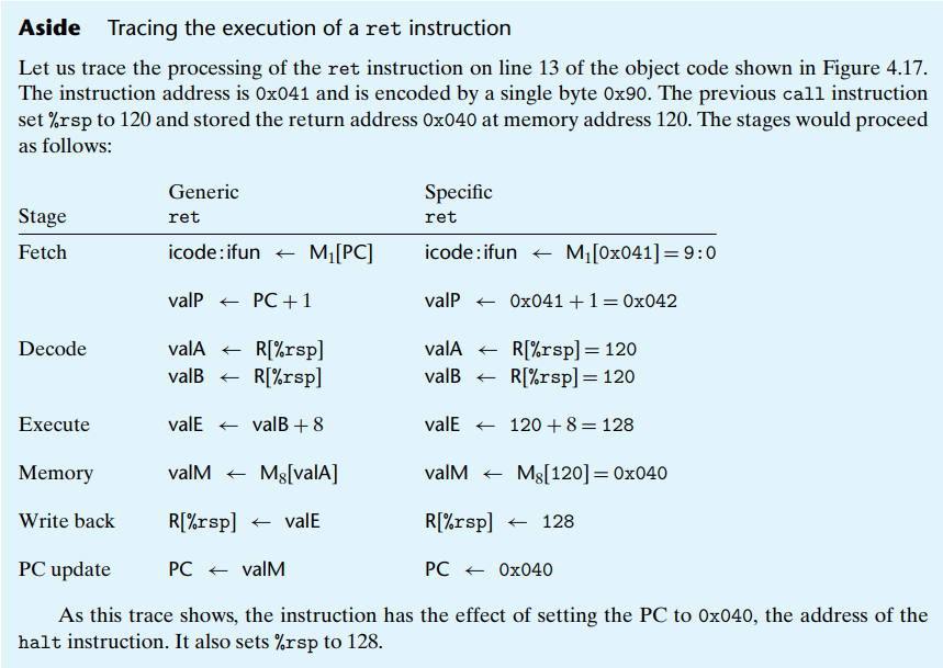
Instructions
callandretis similar topushqandpopq, except that we push and pop program counter values.With instruction call, we push
valP, the address of the instruction that follows the call instruction. During the PC update stage, we set the PC tovalC, the call destination.With instruction
ret, we assignvalM, the value popped from the stack, to the PC in the PC update stage.
2.SEQ Hardware Structure
The following figure shows an abstract view of a hardware structure that performs the six stages:
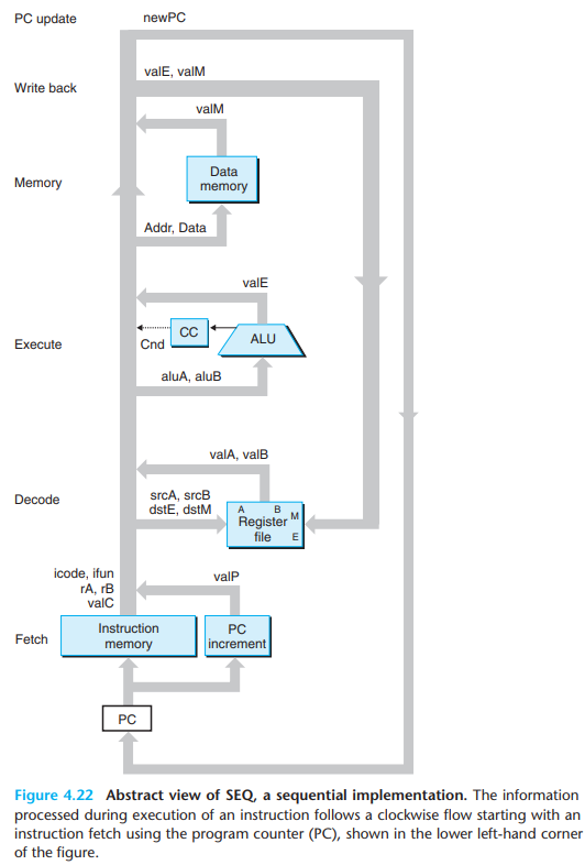
Information then flows along wires(shown grouped together as a heavy gray line), first upward and then around to the right.
The feedback paths coming back down on the right-hand side contain the updated values to write to the register file and the updated program counter.
The six stages are executed as below:
Fetch: Using the program counter register as an address, the instruction memory reads the bytes of an instruction. The PC incrementer computes
valP.Decode: The two register values
valAandvalBare read simultaneously from the read ports A and B.Execute:
The ALU do the operations for different purposes.
The condition code register(CC) holds the three condition code bits. New values for the condition codes are computed by the ALU. The execution of move instruction and the
Cndof the jump instruction is computed based on the CC.
Memory: The data memory reads or writes a word of memory when executing a memory instruction.
- The instruction and data memories access the same memory locations, but for different purposes.
Write Back: The register file has two write ports. Port E is used to write values computed by the ALU, while port M is used to write values read from the data memory.
PC Update: The new value of the program counter is selected to be either
valP, the address of the next instruction,valC, the destination address specified by a call or jump instruction, orvalM, the return address read from memory.
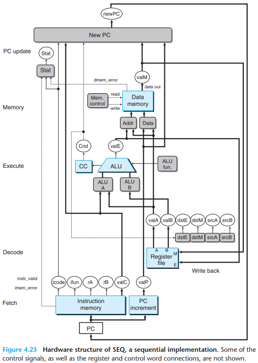
The following figure gives a more detailed view of the hardware design:
3.SEQ Timing
\(a.\)Some basic idea
Combinational logic does not require any sequencing or control-values propagate through a network of logic gates whenever the inputs change.
We assume that reading from a random access memory operates much like combinational logic, with the output word generated based on the address input.
The program counter is loaded with a new instruction address every clock cycle.
The condition code register is loaded only when an integer operation instruction is executed.
The data memory is written only when an
rmmovq,pushq, orcallinstruction is executed.The two write ports of the register file allow two program registers to be updated on every cycle, but we can use the special register ID 0xF as a port address to indicate that no write should be performed for this port.
Principle: The processor never needs to read back the state updated by an instruction in order to complete the processing of this instruction.
\(b.\)Program example
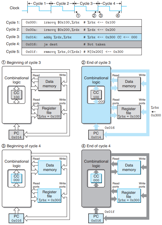
Every time the clock transitions from low to high, the processor begins executing a new instruction.
4.SEQ Stage Implementation
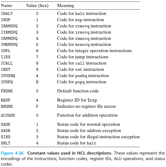
The used constant are shown below:
\(a.\)Fetch stage
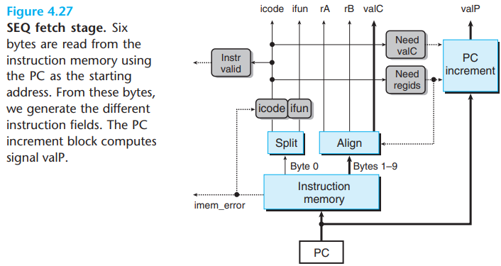
The instruction memory hardware unit reads 10 bytes from memory at a time, using the PC as the address of the first byte(byte 0). This byte is interpreted as the instruction byte and is split(by the unit labeled "Split") into two 4-bit quantities.
The control logic blocks labeled "icode" and "ifun" then compute the instruction and function codes as equaling either the values read from memory or the values corresponding to a nop instruction(as indicated by the signal
imem_error).
Based on the value of icode, we can compute three
1-bit signals:
instr_valid: This signal is used to detect an illegal instruction.need_regids: Does this instruction include a register specifier byte?need_valC: Does this instruction include a constant word?
The signals instr_valid and
imem_error(generated when the instruction address is out of
bounds) are used to generate the status code in the memory
stage.
The HCL description for need_regids and
need_valC are as below:
1 | bool need_regids = |
1 | bool need_valC = |
The remaining 9 bytes read from the instruction memory encode some combination of the register specifier byte and the constant word.
- Byte 1 is split into register specifiers
rAandrBwhen the computed signal need_regids is 1. Ifneed_regidsis 0, both register specifiers are set to 0xF(RNONE).
- Byte 1 is split into register specifiers
The PC incrementer hardware unit generates the signal
valP, based on the current value of the PC, and the two signalsneed_regidsandneed_valC. For PC value \(p\),need_regidsvalue \(r\), andneed_valCvalue \(i\), the incrementer generates the value \(p+1+r+8i\).
\(b.\)Decode and write-back stagess
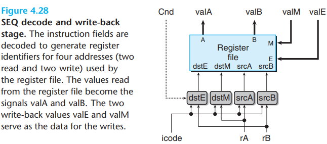
The register file has four ports. It supports up to two simultaneous reads(on ports A and B) and two simultaneous writes(on ports E and M).
Each port has both an address connection and a data connection, where the address connection is a register ID, and the data connection is a set of 64 wires serving as either an output word (for a read port) or an input word (for a write port) of the register file.
The two read ports have address inputs
srcAandsrcB, while the two write ports have address inputsdstEanddstM. The 0xF(RNONE) on an address port indicates that no register should be accessed.
The four blocks at the bottom generate the four different register IDs for the register file based on
icode,rA,rBandCnd.srcAindicates which register should be read to generatevalA, so assrcB.dstEindicates the destination register for write port E, where the computed valuevalEis stored, so asdstM.
The HCL description of srcA and srcB are
as below:
1 | word srcA = [ |
1 | word srcB = [ |
The HCL description of dstM is as below:
1 | word dstM = [ |
\(c.\)Execute stage
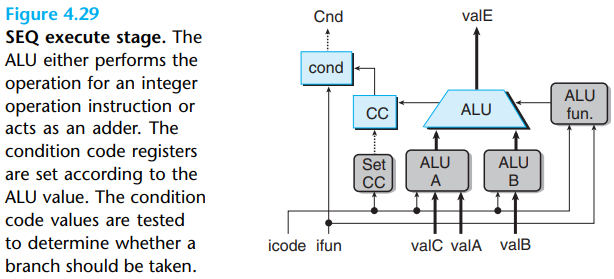
The stage includes ALU, which performs operations based on the setting of
alufunsignal. The ALU output becomes the signalvalE.The value of
aluAcan bevalA,valC, or either ?8 or +8, depending on the instruction type, so asaluB
They can be described by the following HCL code:
1 | word aluA = [ |
1 | word aluB = [ |
- The operations in ALU is mostly an adder. However,
we want it to use the operation encoded in the
ifunfield of the instruction. So we describe the ALU control as below:
1 | word alufun = [ |
- We only want to set the condition codes when an
OPqinstruction is executed. The logic is described in HCL as below:
1 | bool set_cc = icode in { IOPQ }; |
The hardware unit labeled "cond" uses a combination of the condition codes and the function code to determine whether a conditional branch or data transfer should take place.
- It generates the
Cndsignal used both for the setting ofdstEwith conditional moves and in the next PC logic for conditional branches.
- It generates the
By using the Cnd signal, we can describe
dstE as below:
1 | word dstE = [ |
\(d.\)Memory stage
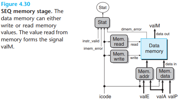
Two control blocks generate the values for the memory address and the memory input data(for write operations).
Two other blocks generate the control signals indicating whether to perform a read or a write operation.
When a read operation is performed, the data memory generates the value
valM.
The HCL description of mem_addr and
mem_data are as below:
1 | word mem_addr = [ |
1 | word mem_data = [ |
- We set the signal
mem_readonly for instructions that read data from memory, so asmem_write:
1 | bool mem_read = icode in { IMRMOVQ, IPOPQ, IRET }; |
1 | bool mem_write = icode in { IRMMOVQ, IPUSHQ, ICALL }; |
- A final function for the memory stage is to compute the status code
Stat. It is generated fromicode,imem_error,instr_validanddmem_error. It's described in HCL as below:
1 | ## Determine instruction status |
\(e.\)PC update stage
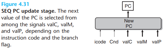
1 | word new_pc = [ |