6.1.Storage Technologies
\(6.1.\)Storage Technologies
1.Random Access Memory
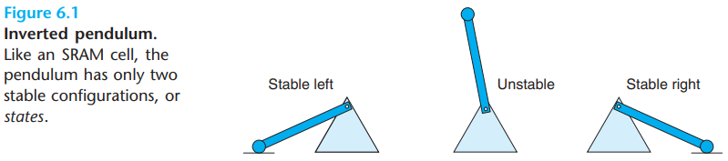
\(a.\)Static RAM
SRAM stores each bit in a bistable memory cell. Each cell is implemented with a six-transistor circuit. This circuit has the property that it can stay indefinitely in either of two different voltage configurations, or states:
\(b.\)Dynamic RAM
DRAM stores each bit as charge on a capacitor. A DRAM memory cell is very sensitive to any disturbance. When the capacitor voltage is disturbed, it will never recover.
\(c.\)Conventional DRAMs
The cells(bits) in a DRAM chip are partitioned into \(d\) supercells, each consisting of \(w\) DRAM cells. A \(d \times w\) DRAM stores a total of \(dw\) bits of information. The supercells are organized as a rectangular array with \(r\) rows and \(c\) columns, where \(rc = d\). Each supercell has an address of the form \((i, j)\), where \(i\) denotes the row and \(j\) denotes the column:
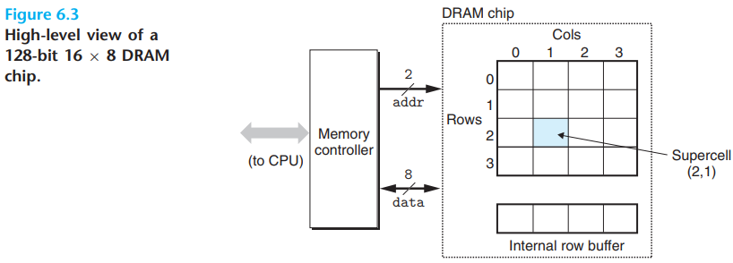
Information flows in and out of the chip via external connectors called pins. Each pin carries a 1-bit signal:
Eight data pins that can transfer 1 byte in or out of the chip.
Two addr pins that carry two-bit row and column supercell addresses.
Each DRAM chip is connected to memory controller.
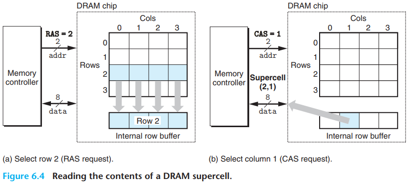
To read the contents of supercell \((i, j)\), the memory controller sends the row address \(i\) to the DRAM first, and then send the column address \(j\). The DRAM responds by sending the contents of supercell \((i, j)\) back to the controller:
The row address \(i\) is called a RAS(row access strobe) request. The column address \(j\) is called a CAS(column access strobe) request.
One reason circuit designers organize DRAMs as two-dimensional arrays instead of linear arrays is to reduce the number of address pins on the chip. However, the address must be sent in two distinct steps, which increases the access time.
\(d.\)Memory modules
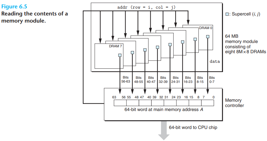
Each supercell stores 1 byte of main memory.
Each 64-bit word at byte address A in main memory is represented by the eight supercells.
To retrieve the word at memory address A, the memory controller converts A to a supercell address \((i, j)\) and sends it to the memory module, which then broadcasts \(i\) and \(j\) to each DRAM.
Main memory can be aggregated by connecting multiple memory modules to the memory controller.
\(e.\)Enhanced DRAMs
A conventional DRAM copies an entire row of supercells into its internal row buffer, uses one, and then discards the rest.
FPM DRAM(Fast Page mode) improves on this by allowing consecutive accesses to the same row to be served directly from the row buffer.
- The initial RAS/CAS request copies row \(i\) into the row buffer and returns the supercell addressed by the CAS. The next three requests then search directly from the row buffer.
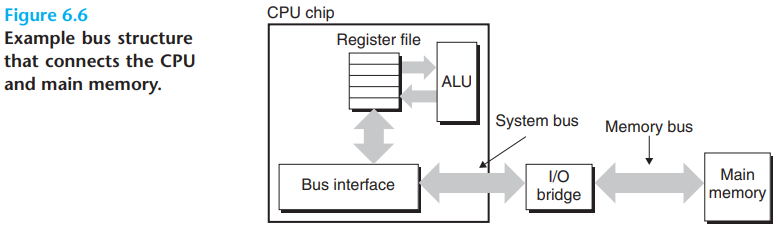
\(e.\)Accessing main memory
\(i.\)Basic structure
Data flows back and forth between the processor and the DRAM main memory over shared electrical conduits called buses.
Each transfer is accomplished with a series of steps called a bus transaction.
The control wires of the bus carry signals that synchronize the transaction and identify what kind of transaction is currently being performed. For example, the operand of the transaction, and the type of the transaction.
\(ii.\)Accessing procedure
Take the following instruction as an example:
1 | movq A, %rax |
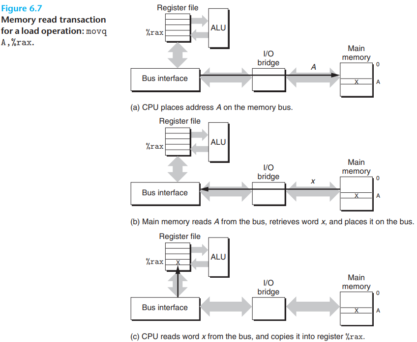
The bus interface initiates a read transaction on the bus.
The CPU places the address A on the system bus. The I/O bridge passes the signal along to the memory bus.
The main memory senses the address signal on the memory bus and fetch the data from DRAM. It writes the data to the memory bus. The I/O bridge translates the memory bus signal into a system bus signal and passes it along to the system bus
The CPU senses the data on the system bus, reads the data from the bus, and copies the data to register
%rax.
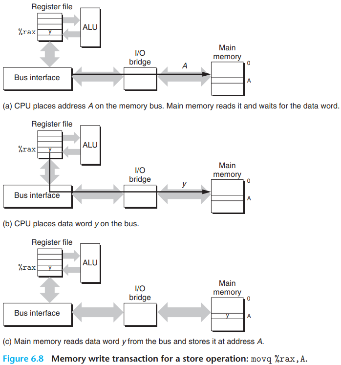
The converse instruction movq %rax,A is similar:
2.Disk Storage
\(a.\)Disk geometry
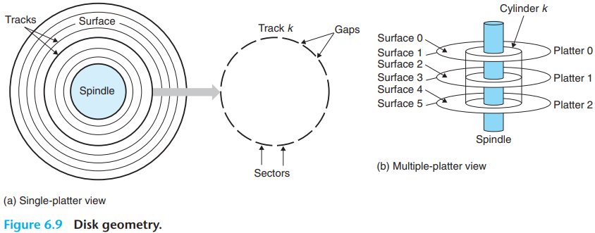
Each surface consists of a collection of concentric rings called tracks.
Each track is partitioned into a collection of sectors.
Sectors are separated by gaps, gaps store formatting bits that identify sectors.
Disk manufacturers describe the geometry of multiple-platter drives in terms of cylinders, where a cylinder is the collection of tracks on all the surfaces that are equidistant from the center of the spindle. For example, if a drive has three platters and six surfaces, and the tracks on each surface are numbered consistently, then cylinder \(k\) is the collection of the six instances of track \(k\).
\(b.\)Disk capacity
Disk capacity is determined by the following technology factors:
Recording density: The number of bits on a track.
Track density: The number of tracks on the radius extending from the center of the platter.
Areal density: The product of the recording density and the track density.
Modern high-capacity disks use a technique known as multiple zone recording, where the set of cylinders is partitioned into disjoint subsets known as recording zones. Each zone consists of a contiguous collection of cylinders. Each track in each cylinder in a zone has the same number of sectors.
The capacity of a disk is given by the following formula:
\[ {Capacity} = \frac{\# {bytes} } {sector} \times \frac{ {average} \# {sectors} } {track} \times \frac{\# {tracks} } {surface} \times \frac{\# {surfaces} } {platter} \times \frac{\# {platters} } {disk} \]
The number of cylinders is identical to \({track} \over {surface}\).
\(e.g.\)What is the capacity of a disk with 3 platters, 15,000 cylinders, an average of 500 sectors per track, and 1,024 bytes per sector?
\(solution\):
\[ Disk\; Capacity = \frac{1,024 \, bytes}{sector} \times \frac{500 \, sectors}{track} \times \frac{15,000 \, tracks}{surface} \times \frac{2 \, surfaces}{platter} \times \frac{3 \, platters}{disk} \]
\(c.\)Disk operations
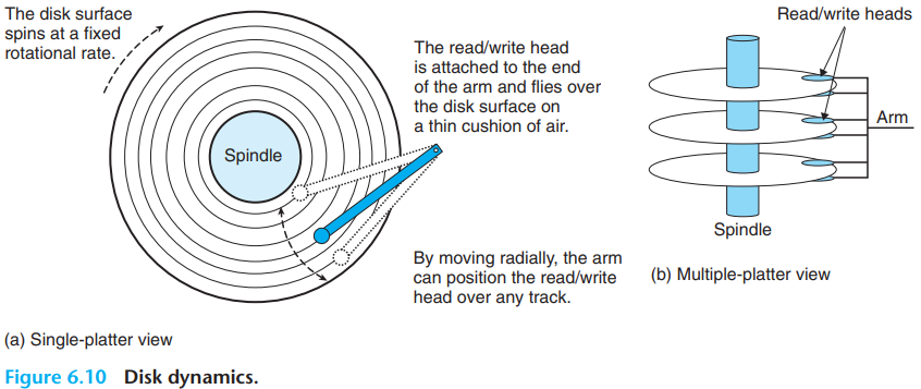
Disks read and write bits stored on the magnetic surface using a read/write head connected to the end of an actuator arm.
- The head can either sense the value of the bit(read the bit) or alter the value of the bit(write the bit).
The disk access time for a sector has three main components: seek time, rotational latency, and transfer time*:
Seek time: It depends on the previous position of the head and the speed that the arm moves across the surface.
Rotational latency:
\[ T_{max \; rotation}={1 \over RPM} \times { {60 \; secs} \over {1 \; min} } \]
- Transfer time:
\[ T_{avg \; transfer} = {1 \over RPM} \times {1 \over {average \; \# \; sector/track} \times { {60 \; secs} \over {1 \; min} }} \]
The \(1 \over {average \; \# \; sector/track}\) is to compute the time cost per sector.
\(d.\)Logical disk blocks
Modern disks present a simple view of their geometry as a sequence of B sector-size logical blocks, numbered 0, 1, ..., B−1.
- The disk controller maintains the mapping between logical block numbers and actual(physical) disk sectors.
When the operating system wants to perform an I/O operation such as reading a disk sector into main memory:
The OS sends a command to the disk controller asking it to read a particular logical block number.
Firmware on the controller performs a fast table lookup that translates the logical block number into a (surface, track, sector) triple that uniquely identifies the corresponding physical sector.
Hardware on the controller interprets this triple to move the heads to the appropriate cylinder.
\(e.\)Accessing disks
Disks are connected to the CPU and main memory using an I/O bus. They are designed to be independent of the underlying CPU.
The CPU issues commands to I/O devices using a technique called memory-mapped I/O.
- In this system, a block of addresses in the address space is reserved for communicating with I/O devices, each of these address is known as an I/O port.
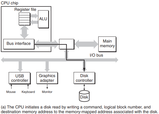
The CPU initiates a disk read by executing three store instructions:
The first of these instructions sends a command word that tells the disk to initiate a read, along with other parameters such as whether to interrupt the CPU when the read is finished.
The second instruction indicates the logical block number that should be read.
The third instruction indicates the main memory address where the contents of the disk sector should be stored.
After it issues the request, the CPU will typically do other work while the disk is performing the read.
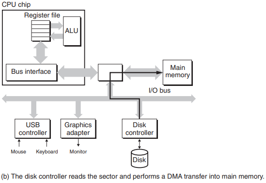
When the disk controller receives the read command from the CPU, it:
- Translates the logical block number to a sector address, reads the contents of the sector, and transfers the contents directly to main memory.
The process is without any involvement of the CPU, and is known as direct memory access(DMA). The transfer of data is known as a DMA transfer.
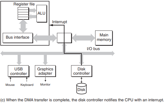
After the DMA transfer is complete and the contents of the disk sector are safely stored in main memory, the disk controller notifies the CPU by sending an interrupt signal to the CPU.
- The basic idea is that an interrupt signals an external pin on the CPU chip. This causes the CPU to stop what it is currently working on and jump to an operating system routine.
3.Solid State Disks
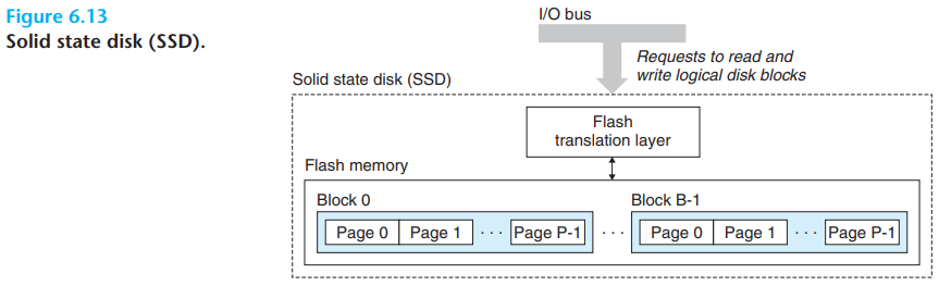
An SSD package plugs into a standard disk slot on the I/O bus and behave like any other disk.
SSD package consists of one or more flash memory chips, which replace the mechanical drive in a conventional rotating disk。
It contains a flash translation layer, which is a hardware/firmware device that plays the same role as a disk controller.
Data are read and written in units of pages. A page can be written only after the entire block to which it belongs has been erased.
Once a block is erased, each page in the block can be written once with no further erasing.
When erasing a block, any pages in the same block with useful data must be copied to a new(erased) block before the write to page p can occur.